|
This is an easy to build, but
nevertheless very accurate and useful digital voltmeter.
It has been designed as a panel meter and can be used in
DC power supplies or anywhere else it is necessary to
have an accurate indication of the voltage present. The
circuit employs the ADC (Analogue to Digital Converter)
I.C. CL7107 made by INTERSIL. This IC incorporates in a
40 pin case all the circuitry necessary to convert an
analogue signal to digital and can drive a series of
four seven segment LED displays directly. The circuits
built into the IC are an analogue to digital converter,
a comparator, a clock, a decoder and a seven segment LED
display driver. The circuit as it is described here can
display any DC voltage in the range of 0-1999 Volts.
Supply Voltage: ............. +/- 5 V (Symmetrical)
Power requirements: ..... 200 mA (maximum)
Measuring range: .......... +/- 0-1,999 VDC in four ranges
Accuracy: ....................... 0.1 %
- Small size
- Easy construction
- Low cost.
- Simple adjustment.
- Easy to read from a distance.
- Few external components.
In order to understand the principle of
operation of the circuit it is necessary to explain how
the ADC IC works. This IC has the following very
important features:
- Great accuracy.
- It is not affected by noise.
- No need for a sample and hold circuit.
- It has a built-in clock.
- It has no need for high accuracy
external components.
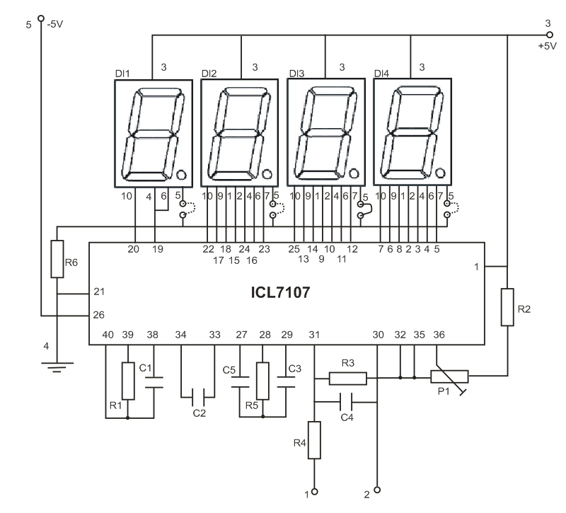
Schematic (fixed 22-2-04)
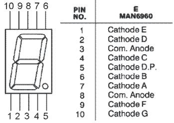
7-segment display pinout MAN6960
An Analogue to Digital Converter, (ADC
from now on) is better known as a dual slope converter
or integrating converter. This type of converter is
generally preferred over other types as it offers
accuracy, simplicity in design and a relative
indifference to noise which makes it very reliable. The
operation of the circuit is better understood if it is
described in two stages. During the first stage and for
a given period the input voltage is integrated, and in
the output of the integrator at the end of this period,
there is a voltage which is directly proportional to the
input voltage. At the end of the preset period the
integrator is fed with an internal reference voltage and
the output of the circuit is gradually reduced until it
reaches the level of the zero reference voltage. This
second phase is known as the negative slope period and
its duration depends on the output of the integrator in
the first period. As the duration of the first operation
is fixed and the length of the second is variable it is
possible to compare the two and this way the input
voltage is in fact compared to the internal reference
voltage and the result is coded and is send to the
display.
All this sounds quite easy but it is in
fact a series of very complex operations which are all
made by the ADC IC with the help of a few external
components which are used to configure the circuit for
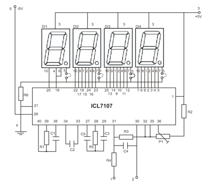
the job. In detail the circuit works as follows. The
voltage to be measured is applied across points 1 and 2
of the circuit and through the circuit R3, R4 and C4 is
finally applied to pins 30 and 31 of the IC. These are
the input of the IC as you can see from its diagram. (IN
HIGH & IN LOW respectively). The resistor R1 together
with C1 are used to set the frequency of the internal
oscillator (clock) which is set at about 48 Hz. At this
clock rate there are about three different readings per
second. The capacitor C2 which is connected between pins
33 and 34 of the IC has been selected to compensate for
the error caused by the internal reference voltage and
also keeps the display steady. The capacitor C3 and the
resistor R5 are together the circuit that does the
integration of the input voltage and at the same time
prevent any division of the input voltage making the
circuit faster and more reliable as the possibility of
error is greatly reduced. The capacitor C5 forces the
instrument to display zero when there is no voltage at
its input. The resistor R2 together with P1 are used to
adjust the instrument during set-up so that it displays
zero when the input is zero. The resistor R6 controls
the current that is allowed to flow through the displays
so that there is sufficient brightness with out damaging
them. The IC as we have already mentioned above is
capable to drive four common anode LED displays. The
three rightmost displays are connected so that they can
display all the numbers from 0 to 9 while the first from
the left can only display the number 1 and when the
voltage is negative the �-� sign. The whole circuit
operates from a symmetrical ρ 5 VDC supply which is
applied at pins 1 (+5 V), 21 (0 V) and 26 (-5 V) of the
IC.
First of all let us consider a few
basics in building electronic circuits on a printed
circuit board. The board is made of a thin insulating
material clad with a thin layer of conductive copper
that is shaped in such a way as to form the necessary
conductors between the various components of the
circuit. The use of a properly designed printed circuit
board is very desirable as it speeds construction up
considerably and reduces the possibility of making
errors. To protect the board during storage from
oxidation and assure it gets to you in perfect condition
the copper is tinned during manufacturing and covered
with a special varnish that protects it from getting
oxidised and also makes soldering easier.
Soldering the components to the board is the only way to
build your circuit and from the way you do it depends
greatly your success or failure. This work is not very
difficult and if you stick to a few rules you should
have no problems. The soldering iron that you use must
be light and its power should not exceed the 25 Watts.
The tip should be fine and must be kept clean at all
times. For this purpose come very handy specially made
sponges that are kept wet and from time to time you can
wipe the hot tip on them to remove all the residues that
tend to accumulate on it.
DO NOT file or sandpaper a dirty or worn
out tip. If the tip cannot be cleaned, replace it. There
are many different types of solder in the market and you
should choose a good quality one that contains the
necessary flux in its core, to assure a perfect joint
every time.
DO NOT use soldering flux apart from
that which is already included in your solder. Too much
flux can cause many problems and is one of the main
causes of circuit malfunction. If nevertheless you have
to use extra flux, as it is the case when you have to
tin copper wires, clean it very thoroughly after you
finish your work.
In order to solder a component correctly
you should do the following:
- Clean the component leads with a small
piece of emery paper.
- Bend them at the correct distance from
the components body and insert the component in its
place on the board.
- You may find sometimes a component
with heavier gauge leads than usual, that are too thick
to enter in the holes of the p.c. board. In this case
use a mini drill to enlarge the holes slightly. Do not
make the holes too large as this is going to make
soldering difficult afterwards.
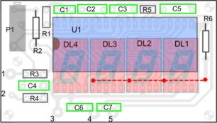
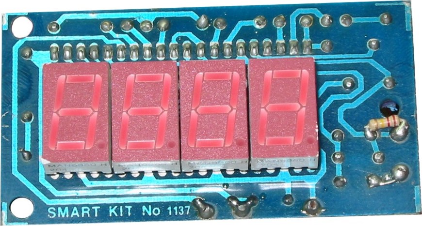
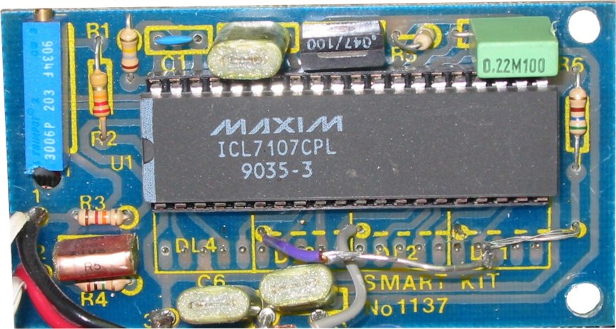
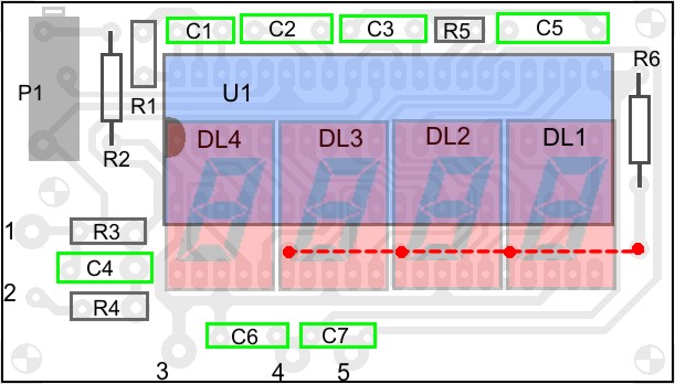
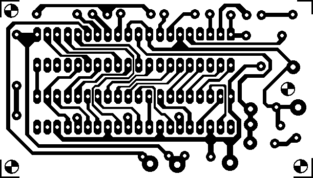
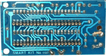
Parts placement
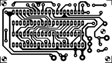
PCB dimensions: 77,6mm x 44,18mm or
scale it at 35%
- Take the hot iron and place its tip on
the component lead while holding the end of the solder
wire at the point where the lead emerges from the board.
The iron tip must touch the lead slightly above the p.c.
board.
- When the solder starts to melt and
flow wait till it covers evenly the area around the hole
and the flux boils and gets out from underneath the
solder. The whole operation should not take more than 5
seconds. Remove the iron and allow the solder to cool
naturally without blowing on it or moving the component.
If everything was done properly the surface of the joint
must have a bright metallic finish and its edges should
be smoothly ended on the component lead and the board
track. If the solder looks dull, cracked, or has the
shape of a blob then you have made a dry joint and you
should remove the solder (with a pump, or a solder wick)
and redo it.
- Take care not to overheat the tracks
as it is very easy to lift them from the board and break
them.
- When you are soldering a sensitive
component it is good practice to hold the lead from the
component side of the board with a pair of long-nose
pliers to divert any heat that could possibly damage the
component.
- Make sure that you do not use more
solder than it is necessary as you are running the risk
of short-circuiting adjacent tracks on the board,
especially if they are very close together.
- When you finish your work, cut off the
excess of the component leads and clean the board
thoroughly with a suitable solvent to remove all flux
residues that may still remain on it.
As it is recommended start working by
identifying the components and separating them in
groups. There are two points in the construction of this
project that you should observe:
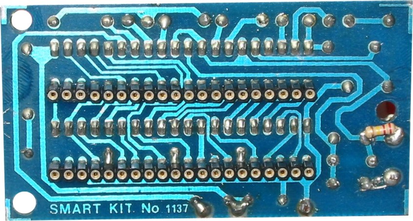
First of all the display ICs are placed
from the copper side of the board and second the jumper
connection which is marked by a dashed line on the
component side at the same place where the displays are
located is not a single jumper but it should be changed
according to the use of the instrument. This jumper is
used to control the decimal point of the display.
If you are going to use the instrument
for only one range you can make the jumper connection
between the rightmost hole on the board and the one
corresponding to the desired position for the decimal
point for your particular application. If you are
planning to use the voltmeter in different ranges you
should use a single pole three position switch to shift
the decimal point to the correct place for the range of
measurement selected. (This switch could preferably be
combined with the switch that is used to actually change
the sensitivity of the instrument).
Apart from this consideration, and the
fact that the small size of the board and the great
number of joints on it which calls for a very fine
tipped soldering iron, the construction of the project
is very straightforward.
Insert the IC socket and solder it in
place, solder the pins, continue with the resistors the
capacitors and the multi-turn trimmer P1. Turn the board
over and very carefully solder the display ICs from the
copper side of the board. Remember to inspect the joints
of the base of the IC as one row will be covered by the
displays and will be impossible to see any mistake that
you may have made after you have soldered the displays
into place.
The value of R3 controls in fact the
range of measurement of the voltmeter and if you provide
for some means to switch different resistors in its
place you can use the instrument over a range of
voltages.
For the replacement resistors follow the
table below:
0 - 2 V ............ R3 = 0 ohm 1%
0 - 20 V ........... R3 = 1.2 Kohm 1%
0 - 200 V .......... R3 = 12 Kohm 1%
0 - 2000 V ......... R3 = 120 Kohm 1%
When you have finished all the soldering
on the board and you are sure that everything is OK you
can insert the IC in its place. The IC is CMOS and is
very sensitive to static electricity. It comes wrapped
in aluminium foil to protect it from static discharges
and it should be handled with great care to avoid
damaging it. Try to avoid touching its pins with your
hands and keep the circuit and your body at ground
potential when you insert it in its place.
Connect the circuit to a suitable power
supply ρ 5 VDC and turn the supply on. The displays
should light immediately and should form a number. Short
circuit the input (0 V) and adjust the trimmer P1 until
the display indicates exactly �0�.
R1 = 180k
P1 = 20k trimmer multi turn
R2 = 22k
U1 = ICL 7107
R3 = 12k
LD1,2,3,4 = MAN 6960 common
anode led displays
R4 = 1M
R5 = 470k
R6 = 560 Ohm
C1 = 100pF
C2, C6, C7 = 100nF
C3 = 47nF
C4 = 10nF
C5 = 220nF
Check your work for possible dry joints,
bridges across adjacent tracks or soldering flux
residues that usually cause problems.
Check again all the external connections
to and from the circuit to see if there is a mistake
there.
- See that there are no components
missing or inserted in the wrong places.
- Make sure that all the polarised
components have been soldered the right way round. -
Make sure the supply has the correct voltage and is
connected the right way round to your circuit.
- Check your project for faulty or
damaged components.
|