NOR gate S-R latch
PARTS AND MATERIALS
-
4001 quad NOR gate (Radio Shack catalog #
276-2401)
-
Eight-position DIP switch (Radio Shack
catalog # 275-1301)
-
Ten-segment bargraph LED (Radio Shack
catalog # 276-081)
-
One 6 volt battery
-
Two 10 kΩ resistors
-
Two 470 Ω resistors
-
Two 100 Ω resistors
Caution! The 4001 IC is CMOS, and
therefore sensitive to static electricity!
CROSS-REFERENCES
Lessons In Electric Circuits, Volume
4, chapter 3: "Logic Gates"
Lessons In Electric Circuits, Volume
4, chapter 10: "Multivibrators"
LEARNING OBJECTIVES
-
The effects of positive feedback in a
digital circuit
-
What is meant by the "invalid" state of a
latch circuit
-
What a race condition is in a
digital circuit
-
The importance of valid "high" CMOS signal
voltage levels
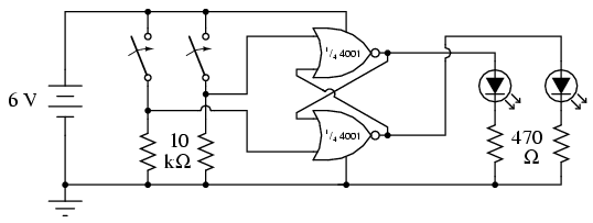
SCHEMATIC DIAGRAM
ILLUSTRATION
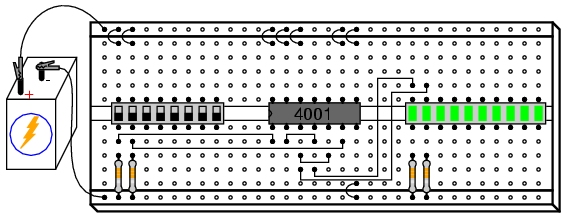
INSTRUCTIONS
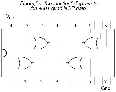
The 4001 integrated circuit is a CMOS quad
NOR gate, identical in input, output, and power supply pin
assignments to the 4011 quad NAND gate. Its "pinout," or
"connection," diagram is as such:
When two NOR gates are cross-connected as
shown in the schematic diagram, there will be positive
feedback from output to input. That is, the output signal
tends to maintain the gate in its last output state. Just as
in op-amp circuits, positive feedback creates hysteresis.
This tendency for the circuit to remain in its last output
state gives it a sort of "memory." In fact, there are
solid-state computer memory technologies based on circuitry
like this!
If we designate the left switch as the "Set"
input and the right switch as the "Reset," the left LED will
be the "Q" output and the right LED the "Q-not" output. With
the Set input "high" (switch on) and the Reset input "low,"
Q will go "high" and Q-not will go "low." This is known as
the set state of the circuit. Making the Reset input
"high" and the Set input "low" reverses the latch circuit's
output state: Q "low" and Q-not "high." This is known as the
reset state of the circuit. If both inputs are placed
into the "low" state, the circuit's Q and Q-not outputs will
remain in their last states, "remembering" their prior
settings. This is known as the latched state of the
circuit.
Because the outputs have been designated "Q"
and "Q-not," it is implied that their states will always be
complementary (opposite). Thus, if something were to happen
that forced both outputs to the same state, we would
be inclined to call that mode of the circuit "invalid." This
is exactly what will happen if we make both Set and Reset
inputs "high:" both Q and Q-not outputs will be forced to
the same "low" logic state. This is known as the invalid
or illegal state of the circuit, not because
something has gone wrong, but because the outputs have
failed to meet the expectations established by their labels.
Since the "latched" state is a hysteretic
condition whereby the last output states are "remembered,"
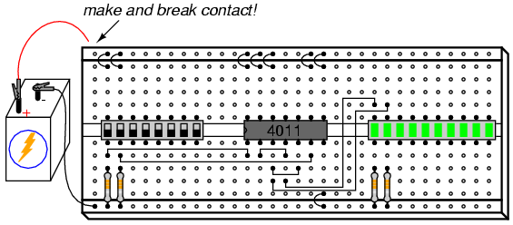
one might wonder what will happen if the circuit powers up
this way, with no previous state to hold. To
experiment, place both switches in their off positions,
making both Set and Reset inputs low, then disconnect one of
the battery wires from the breadboard. Then, quickly make
and break contact between that battery wire and its proper
connection point on the breadboard, noting the status of the
two LEDs as the circuit is powered up again and again:
When a latch circuit such as this is powered
up into its "latched" state, the gates race against each
other for control. Given the "low" inputs, both gates try to
output "high" signals. If one of the gates reaches its
"high" output state before the other, that "high" state will
be fed back to the other gate's input to force its output
"low," and the race is won by the faster gate.
Invariably, one gate wins the race, due to
internal variations between gates in the chip, and/or
external resistances and capacitances that act to delay one
gate more than the other. What this usually means is that
the circuit tends to power up in the same mode, over and
over again. However, if you are persistent in your powering/unpowering
cycles, you should see at least a few times where the latch
circuit powers up latched in the opposite state from
normal.
Race conditions are generally undesirable in
any kind of system, as they lead to unpredictable operation.
They can be particularly troublesome to locate, as this
experiment shows, because of the unpredictability they
create. Imagine a scenario, for instance, where one of the
two NOR gates was exceptionally slow-acting, due to a defect
in the chip. This handicap would cause the other gate to win
the power-up race every time. In other words, the circuit
will be very predictable on power-up with both inputs "low."
However, suppose that the unusual chip were to be replaced
by one with more evenly matched gates, or by a chip where
the other NOR gate were consistently slower. Normal
circuit behavior is not supposed to change when a component
is replaced, but if race conditions are present, a change of
components may very well do just that.
Due to the inherent race tendency of an S-R
latch, one should not design a circuit with the expectation
of a consistent power-up state, but rather use external
means to "force" the race so that the desired gate always
"wins."
An interesting modification to try in this
circuit is to replace one of the 470 Ω LED "dropping"
resistors with a lower-value unit, such as 100 Ω. The
obvious effect of this alteration will be increased LED
brightness, as more current is allowed through. A
not-so-obvious effect will also result, and it is this
effect which holds great learning value. Try replacing one
of the 470 Ω resistors with a 100 Ω resistor, and operate
the input signal switches through all four possible setting
combinations, noting the behavior of the circuit.
You should note that the circuit refuses to
latch in one of its states (either Set or Reset), but only
in the other state, when the input switches are both set
"low" (the "latch" mode). Why is this? Take a voltmeter and
measure the output voltage of the gate whose output is
"high" when both inputs are "low." Note this voltage
indication, then set the input switches in such a way that
the other state (either Reset or Set) is forced, and
measure the output voltage of the other gate when its output
is "high." Note the difference between the two gate output
voltage levels, one gate loaded by an LED with a 470 Ω
resistor, and the other loaded by an LED with a 100 Ω
resistor. The one loaded down by the "heavier" load (100 Ω
resistor) will be much less: so much less that this voltage
will not be interpreted by the other NOR gate's input as a
"high" signal at all as it is fed back! All logic gates have
permissible "high" and "low" input signal voltage ranges,
and if the voltage of a digital signal falls outside this
permissible range, it might not be properly interpreted by
the receiving gate. In a latch circuit such as this, which
depends on a solid "high" signal fed back from the output of
one gate to the input of the other, a "weak" signal will not
be able to maintain the positive feedback necessary to keep
the circuit latched in one of its states.
This is one reason I favor the use of a
voltmeter as a logic "probe" for determining digital signal
levels, rather than an actual logic probe with "high" and
"low" lights. A logic probe may not indicate the presence of
a "weak" signal, whereas a voltmeter definitely will by
means of its quantitative indication. This type of problem,
common in circuits where different "families" of integrated
circuits are mixed (TTL and CMOS, for example), can only be
found with test equipment providing quantitative
measurements of signal level. |
