Class B audio amplifier
PARTS AND MATERIALS
-
Four 6 volt batteries
-
Dual operational amplifier, model TL082
recommended (Radio Shack catalog # 276-1715)
-
One NPN power transistor in a TO-220
package -- (Radio Shack catalog # 276-2020 or equivalent)
-
One PNP power transistor in a TO-220
package -- (Radio Shack catalog # 276-2027 or equivalent)
-
One 1N914 switching diode (Radio Shack
catalog # 276-1620)
-
One capacitor, 47 �F electrolytic, 35 WVDC
(Radio Shack catalog # 272-1015 or equivalent)
-
Two capacitors, 0.22 �F, non-polarized
(Radio Shack catalog # 272-1070)
-
One 10 kΩ potentiometer, linear taper
(Radio Shack catalog # 271-1715)
Be sure to use an op-amp that has a high
slew rate. Avoid the LM741 or LM1458 for this reason.
The closer matched the two transistors are,
the better. If possible, try to obtain TIP41 and TIP42
transistors, which are closely matched NPN and PNP power
transistors with dissipation ratings of 65 watts each. If
you cannot get a TIP41 NPN transistor, the TIP3055
(available from Radio Shack) is a good substitute. Do not
use very large (i.e. TO-3 case) power transistors, as the
op-amp may have trouble driving enough current to their
bases for good operation.
CROSS-REFERENCES
Lessons In Electric Circuits, Volume
3, chapter 4: "Bipolar Junction Transistors"
Lessons In Electric Circuits, Volume
3, chapter 8: "Operational Amplifiers"
LEARNING OBJECTIVES
-
How to build a "push-pull" class B
amplifier using complementary bipolar transistors
-
The effects of "crossover distortion" in a
push-pull amplifier circuit
-
Using negative feedback via an op-amp to
correct circuit nonlinearities
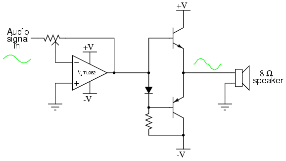
SCHEMATIC DIAGRAM

ILLUSTRATION

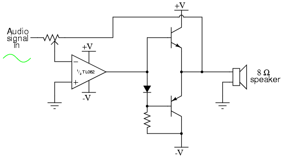
INSTRUCTIONS
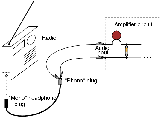
This project is an audio amplifier suitable
for amplifying the output signal from a small radio, tape
player, CD player, or any other source of audio signals. For
stereo operation, two identical amplifiers must be built,
one for the left channel and other for the right channel. To
obtain an input signal for this amplifier to amplify, just
connect it to the output of a radio or other audio device
like this:
This amplifier circuit also works well in
amplifying "line-level" audio signals from high-quality,
modular stereo components. It provides a surprising amount
of sound power when played through a large speaker, and may
be run without heat sinks on the transistors (though you
should experiment with it a bit before deciding to forego
heat sinks, as the power dissipation varies according to the
type of speaker used).
The goal of any amplifier circuit is to
reproduce the input waveshape as accurately as possible.
Perfect reproduction is impossible, of course, and any
differences between the output and input waveshapes is known
as distortion. In an audio amplifier, distortion may
cause unpleasant tones to be superimposed on the true sound.
There are many different configurations of audio amplifier
circuitry, each with its own advantages and disadvantages.
This particular circuit is called a "class B," push-pull
circuit.
Most audio "power" amplifiers use a class B
configuration, where one transistor provides power to the
load during one-half of the waveform cycle (it pushes)
and a second transistor provides power to the load for the
other half of the cycle (it pulls). In this scheme,
neither transistor remains "on" for the entire cycle, giving
each one a time to "rest" and cool during the waveform
cycle. This makes for a power-efficient amplifier circuit,
but leads to a distinct type of nonlinearity known as
"crossover distortion."
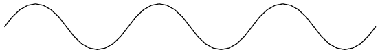
Shown here is a sine-wave shape, equivalent
to a constant audio tone of constant volume:
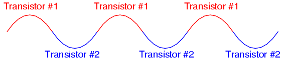
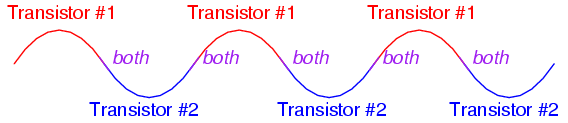
In a push-pull amplifier circuit, the two
transistors take turns amplifying the alternate half-cycles
of the waveform like this:
If the "hand-off" between the two
transistors is not precisely synchronized, though, the
amplifier's output waveform may look something like this
instead of a pure sine wave:
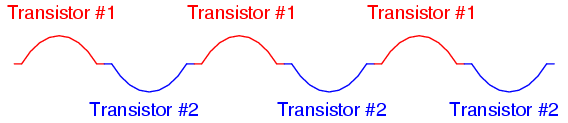
Here, distortion results from the fact that
there is a delay between the time one transistor turns off
and the other transistor turns on. This type of distortion,
where the waveform "flattens" at the crossover point between
positive and negative half-cycles, is called crossover
distortion. One common method of mitigating crossover
distortion is to bias the transistors so that their
turn-on/turn-off points actually overlap, so that both
transistors are in a state of conduction for a brief moment
during the crossover period:
This form of amplification is technically
known as class AB rather than class B, because each
transistor is "on" for more than 50% of the time during a
complete waveform cycle. The disadvantage to doing this,
though, is increased power consumption of the amplifier
circuit, because during the moments of time where both
transistors are conducting, there is current conducted
through the transistors that is not going through the
load, but is merely being "shorted" from one power supply
rail to the other (from -V to +V). Not only is this a waste
of energy, but it dissipates more heat energy in the
transistors. When transistors increase in temperature, their
characteristics change (Vbe forward voltage drop,
β, junction resistances, etc.), making proper biasing
difficult.
In this experiment, the transistors operate
in pure class B mode. That is, they are never conducting at
the same time. This saves energy and decreases heat
dissipation, but lends itself to crossover distortion. The
solution taken in this circuit is to use an op-amp with
negative feedback to quickly drive the transistors through
the "dead" zone producing crossover distortion and reduce
the amount of "flattening" of the waveform during crossover.
The first (leftmost) op-amp shown in the
schematic diagram is nothing more than a buffer. A buffer
helps to reduce the loading of the input capacitor/resistor
network, which has been placed in the circuit to filter out
any DC bias voltage out of the input signal, preventing any
DC voltage from becoming amplified by the circuit and sent
to the speaker where it might cause damage. Without the
buffer op-amp, the capacitor/resistor filtering circuit
reduces the low-frequency ("bass") response of the
amplifier, and accentuates the high-frequency ("treble").
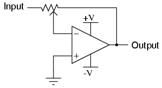
The second op-amp functions as an inverting
amplifier whose gain is controlled by the 10 kΩ
potentiometer. This does nothing more than provide a volume
control for the amplifier. Usually, inverting op-amp
circuits have their feedback resistor(s) connected directly
from the op-amp output terminal to the inverting input
terminal like this:
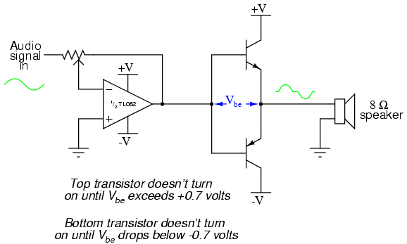
If we were to use the resulting output
signal to drive the base terminals of the push-pull
transistor pair, though, we would experience significant
crossover distortion, because there would be a "dead" zone
in the transistors' operation as the base voltage went from
+ 0.7 volts to - 0.7 volts:
If you have already constructed the
amplifier circuit in its final form, you may simplify it to
this form and listen to the difference in sound quality. If
you have not yet begun construction of the circuit, the
schematic diagram shown above would be a good starting
point. It will amplify an audio signal, but it will sound
horrible!
The reason for the crossover distortion is
that when the op-amp output signal is between + 0.7 volts
and - 0.7 volts, neither transistor will be conducting, and
the output voltage to the speaker will be 0 volts for the
entire 1.4 volts span of base voltage swing. Thus, there is
a "zone" in the input signal range where no change in
speaker output voltage will occur. Here is where intricate
biasing techniques are usually introduced to the circuit to
reduce this 1.4 volt "gap" in transistor input signal
response. Usually, something like this is done:

The two series-connected diodes will drop
approximately 1.4 volts, equivalent to the combined Vbe
forward voltage drops of the two transistors, resulting in a
scenario where each transistor is just on the verge of
turning on when the input signal is zero volts, eliminating
the 1.4 volt "dead" signal zone that existed before.
Unfortunately, though, this solution is not
perfect: as the transistors heat up from conducting power to
the load, their Vbe forward voltage drops will
decrease from 0.7 volts to something less, such as 0.6 volts
or 0.5 volts. The diodes, which are not subject to the same
heating effect because they do not conduct any substantial
current, will not experience the same change in forward
voltage drop. Thus, the diodes will continue to provide the
same 1.4 volt bias voltage even though the transistors
require less bias voltage due to heating. The result will be
that the circuit drifts into class AB operation, where
both transistors will be in a state of conduction part
of the time. This, of course, will result in more heat
dissipation through the transistors, exacerbating the
problem of forward voltage drop change.
A common solution to this problem is the
insertion of temperature-compensation "feedback" resistors
in the emitter legs of the push-pull transistor circuit:
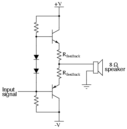
This solution doesn't prevent simultaneous
turn-on of the two transistors, but merely reduces the
severity of the problem and prevents thermal runaway. It
also has the unfortunate effect of inserting resistance in
the load current path, limiting the output current of the
amplifier. The solution I opted for in this experiment is
one that capitalizes on the principle of op-amp negative
feedback to overcome the inherent limitations of the
push-pull transistor output circuit. I use one diode to
provide a 0.7 volt bias voltage for the push-pull pair. This
is not enough to eliminate the "dead" signal zone, but it
reduces it by at least 50%:
Since the voltage drop of a single diode
will always be less than the combined voltage drops of the
two transistors' base-emitter junctions, the transistors can
never turn on simultaneously, thereby preventing class AB
operation. Next, to help get rid of the remaining crossover
distortion, the feedback signal of the op-amp is taken from
the output terminal of the amplifier (the transistors'
emitter terminals) like this:
The op-amp's function is to output whatever
voltage signal it has to in order to keep its two input
terminals at the same voltage (0 volts differential). By
connecting the feedback wire to the emitter terminals of the
push-pull transistors, the op-amp has the ability to sense
any "dead" zone where neither transistor is conducting, and
output an appropriate voltage signal to the bases of the
transistors to quickly drive them into conduction again to
"keep up" with the input signal waveform. This requires an
op-amp with a high slew rate (the ability to produce
a fast-rising or fast-falling output voltage), which is why
the TL082 op-amp was specified for this circuit. Slower
op-amps such as the LM741 or LM1458 may not be able to keep
up with the high dv/dt (voltage rate-of-change over time,
also known as de/dt) necessary for low-distortion
operation.
Only a couple of capacitors are added to
this circuit to bring it into its final form: a 47 �F
capacitor connected in parallel with the diode helps to keep
the 0.7 volt bias voltage constant despite large voltage
swings in the op-amp's output, while a 0.22 �F capacitor
connected between the base and emitter of the NPN transistor
helps reduce crossover distortion at low volume settings:
|
