Up until this point, our analysis of transistor logic
circuits has been limited to the TTL design paradigm, whereby bipolar
transistors are used, and the general strategy of floating inputs being
equivalent to "high" (connected to Vcc) inputs -- and
correspondingly, the allowance of "open-collector" output stages -- is
maintained. This, however, is not the only way we can build logic gates.
Field-effect transistors, particularly the insulated-gate variety, may be
used in the design of gate circuits. Being voltage-controlled rather than
current-controlled devices, IGFETs tend to allow very simple circuit
designs. Take for instance, the following inverter circuit built using P-
and N-channel IGFETs:
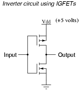
Notice the "Vdd" label on the positive power supply terminal.
This label follows the same convention as "Vcc" in TTL circuits:
it stands for the constant voltage applied to the drain of a field effect
transistor, in reference to ground.
Let's connect this gate circuit to a power source and input switch, and
examine its operation. Please note that these IGFET transistors are E-type
(Enhancement-mode), and so are normally-off devices. It takes an
applied voltage between gate and drain (actually, between gate and
substrate) of the correct polarity to bias them on.
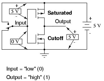
The upper transistor is a P-channel IGFET. When the channel (substrate)
is made more positive than the gate (gate negative in reference to the
substrate), the channel is enhanced and current is allowed between source
and drain. So, in the above illustration, the top transistor is turned on.
The lower transistor, having zero voltage between gate and substrate
(source), is in its normal mode: off. Thus, the action of these two
transistors are such that the output terminal of the gate circuit has a
solid connection to Vdd and a very high resistance connection to
ground. This makes the output "high" (1) for the "low" (0) state of the
input.
Next, we'll move the input switch to its other position and see what
happens:
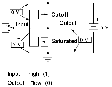
Now the lower transistor (N-channel) is saturated because it has
sufficient voltage of the correct polarity applied between gate and
substrate (channel) to turn it on (positive on gate, negative on the
channel). The upper transistor, having zero voltage applied between its gate
and substrate, is in its normal mode: off. Thus, the output of this
gate circuit is now "low" (0). Clearly, this circuit exhibits the behavior
of an inverter, or NOT gate.
Using field-effect transistors instead of bipolar transistors has greatly
simplified the design of the inverter gate. Note that the output of this
gate never floats as is the case with the simplest TTL circuit: it has a
natural "totem-pole" configuration, capable of both sourcing and sinking
load current. Key to this gate circuit's elegant design is the
complementary use of both P- and N-channel IGFETs. Since IGFETs are more
commonly known as MOSFETs (Metal-Oxide-Semiconductor
Field Effect Transistor), and this circuit uses both P-
and N-channel transistors together, the general classification given to gate
circuits like this one is CMOS: Complementary Metal
Oxide Semiconductor.
CMOS circuits aren't plagued by the inherent nonlinearities of the
field-effect transistors, because as digital circuits their transistors
always operate in either the saturated or cutoff modes and
never in the active mode. Their inputs are, however, sensitive to
high voltages generated by electrostatic (static electricity) sources, and
may even be activated into "high" (1) or "low" (0) states by spurious
voltage sources if left floating. For this reason, it is inadvisable to
allow a CMOS logic gate input to float under any circumstances. Please note
that this is very different from the behavior of a TTL gate where a floating
input was safely interpreted as a "high" (1) logic level.
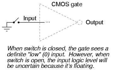
This may cause a problem if the input to a CMOS logic gate is driven by a
single-throw switch, where one state has the input solidly connected to
either Vdd or ground and the other state has the input floating
(not connected to anything):
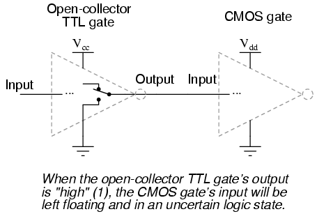
Also, this problem arises if a CMOS gate input is being driven by an
open-collector TTL gate. Because such a TTL gate's output floats when it
goes "high" (1), the CMOS gate input will be left in an uncertain state:
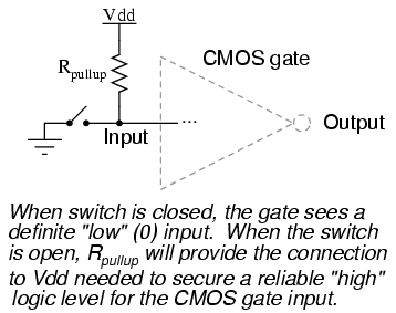
Fortunately, there is an easy solution to this dilemma, one that is used
frequently in CMOS logic circuitry. Whenever a single-throw switch (or any
other sort of gate output incapable of both sourcing and sinking
current) is being used to drive a CMOS input, a resistor connected to either
Vdd or ground may be used to provide a stable logic level for the
state in which the driving device's output is floating. This resistor's
value is not critical: 10 kΩ is usually sufficient. When used to provide a
"high" (1) logic level in the event of a floating signal source, this
resistor is known as a pullup resistor:
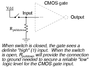
When such a resistor is used to provide a "low" (0) logic level in the
event of a floating signal source, it is known as a pulldown resistor.
Again, the value for a pulldown resistor is not critical:
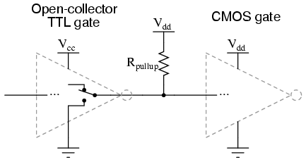
Because open-collector TTL outputs always sink, never source, current,
pullup resistors are necessary when interfacing such an output to a
CMOS gate input:
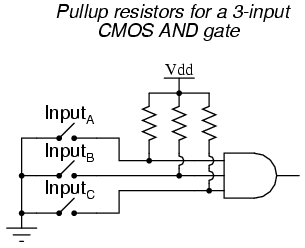
Although the CMOS gates used in the preceding examples were all inverters
(single-input), the same principle of pullup and pulldown resistors applies
to multiple-input CMOS gates. Of course, a separate pullup or pulldown
resistor will be required for each gate input:
This brings us to the next question: how do we design multiple-input CMOS
gates such as AND, NAND, OR, and NOR? Not surprisingly, the answer(s) to
this question reveal a simplicity of design much like that of the CMOS
inverter over its TTL equivalent.
For example, here is the schematic diagram for a CMOS NAND gate:
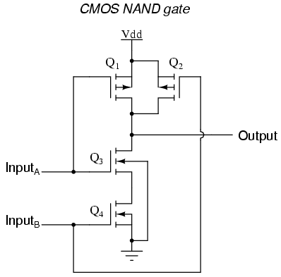
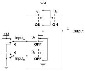
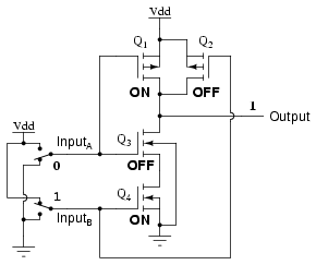
Notice how transistors Q1 and Q3 resemble the
series-connected complementary pair from the inverter circuit. Both are
controlled by the same input signal (input A), the upper transistor turning
off and the lower transistor turning on when the input is "high" (1), and
visa-versa. Notice also how transistors Q2 and Q4 are
similarly controlled by the same input signal (input B), and how they will
also exhibit the same on/off behavior for the same input logic levels. The
upper transistors of both pairs (Q1 and Q2) have their
source and drain terminals paralleled, while the lower transistors (Q3
and Q4) are series-connected. What this means is that the output
will go "high" (1) if either top transistor saturates, and will go
"low" (0) only if both lower transistors saturate. The following
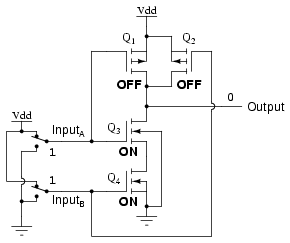
sequence of illustrations shows the behavior of this NAND gate for all four
possibilities of input logic levels (00, 01, 10, and 11):
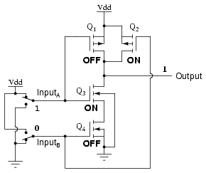
>
As with the TTL NAND gate, the CMOS NAND gate circuit may be used as the
starting point for the creation of an AND gate. All that needs to be added
is another stage of transistors to invert the output signal:

A CMOS NOR gate circuit uses four MOSFETs just like the NAND gate, except
that its transistors are differently arranged. Instead of two paralleled
sourcing (upper) transistors connected to Vdd and two
series-connected sinking (lower) transistors connected to ground, the
NOR gate uses two series-connected sourcing transistors and two
parallel-connected sinking transistors like this:
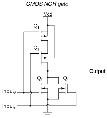
As with the NAND gate, transistors Q1 and Q3 work
as a complementary pair, as do transistors Q2 and Q4.
Each pair is controlled by a single input signal. If either input A
or input B are "high" (1), at least one of the lower transistors (Q3
or Q4) will be saturated, thus making the output "low" (0). Only
in the event of both inputs being "low" (0) will both lower
transistors be in cutoff mode and both upper transistors be saturated, the
conditions necessary for the output to go "high" (1). This behavior, of
course, defines the NOR logic function.
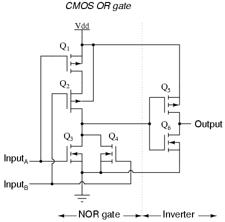
The OR function may be built up from the basic NOR gate with the addition
of an inverter stage on the output:
Since it appears that any gate possible to construct using TTL technology
can be duplicated in CMOS, why do these two "families" of logic design still
coexist? The answer is that both TTL and CMOS have their own unique
advantages.
First and foremost on the list of comparisons between TTL and CMOS is the
issue of power consumption. In this measure of performance, CMOS is the
unchallenged victor. Because the complementary P- and N-channel MOSFET pairs
of a CMOS gate circuit are (ideally) never conducting at the same time,
there is little or no current drawn by the circuit from the Vdd
power supply except for what current is necessary to source current to a
load. TTL, on the other hand, cannot function without some current drawn at
all times, due to the biasing requirements of the bipolar transistors from
which it is made.
There is a caveat to this advantage, though. While the power dissipation
of a TTL gate remains rather constant regardless of its operating state(s),
a CMOS gate dissipates more power as the frequency of its input signal(s)
rises. If a CMOS gate is operated in a static (unchanging) condition, it
dissipates zero power (ideally). However, CMOS gate circuits draw transient
current during every output state switch from "low" to "high" and
visa-versa. So, the more often a CMOS gate switches modes, the more often it
will draw current from the Vdd supply, hence greater power
dissipation at greater frequencies.
A CMOS gate also draws much less current from a driving gate output than
a TTL gate because MOSFETs are voltage-controlled, not current-controlled,
devices. This means that one gate can drive many more CMOS inputs than TTL
inputs. The measure of how many gate inputs a single gate output can drive
is called fanout.
Another advantage that CMOS gate designs enjoy over TTL is a much wider
allowable range of power supply voltages. Whereas TTL gates are restricted
to power supply (Vcc) voltages between 4.75 and 5.25 volts, CMOS
gates are typically able to operate on any voltage between 3 and 15 volts!
The reason behind this disparity in power supply voltages is the respective
bias requirements of MOSFET versus bipolar junction transistors. MOSFETs are
controlled exclusively by gate voltage (with respect to substrate), whereas
BJTs are current-controlled devices. TTL gate circuit resistances are
precisely calculated for proper bias currents assuming a 5 volt regulated
power supply. Any significant variations in that power supply voltage will
result in the transistor bias currents being incorrect, which then results
in unreliable (unpredictable) operation. The only effect that variations in
power supply voltage have on a CMOS gate is the voltage definition of a
"high" (1) state. For a CMOS gate operating at 15 volts of power supply
voltage (Vdd), an input signal must be close to 15 volts in order
to be considered "high" (1). The voltage threshold for a "low" (0) signal
remains the same: near 0 volts.
One decided disadvantage of CMOS is slow speed, as compared to TTL. The
input capacitances of a CMOS gate are much, much greater than that of a
comparable TTL gate -- owing to the use of MOSFETs rather than BJTs -- and
so a CMOS gate will be slower to respond to a signal transition (low-to-high
or visa-versa) than a TTL gate, all other factors being equal. The RC time
constant formed by circuit resistances and the input capacitance of the gate
tend to impede the fast rise- and fall-times of a digital logic level,
thereby degrading high-frequency performance.
A strategy for minimizing this inherent disadvantage of CMOS gate
circuitry is to "buffer" the output signal with additional transistor
stages, to increase the overall voltage gain of the device. This provides a
faster-transitioning output voltage (high-to-low or low-to-high) for an
input voltage slowly changing from one logic state to another. Consider this
example, of an "unbuffered" NOR gate versus a "buffered," or B-series,
NOR gate:
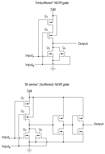
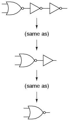
In essence, the B-series design enhancement adds two inverters to the
output of a simple NOR circuit. This serves no purpose as far as digital
logic is concerned, since two cascaded inverters simply cancel:
However, adding these inverter stages to the circuit does serve the
purpose of increasing overall voltage gain, making the output more sensitive
to changes in input state, working to overcome the inherent slowness caused
by CMOS gate input capacitance.
REVIEW: CMOS logic gates are made of IGFET (MOSFET) transistors rather than
bipolar junction transistors. CMOS gate inputs are sensitive to static electricity. They may be
damaged by high voltages, and they may assume any logic level if left
floating. Pullup and pulldown resistors are used to prevent a CMOS
gate input from floating if being driven by a signal source capable only
of sourcing or sinking current. CMOS gates dissipate far less power than equivalent TTL gates, but
their power dissipation increases with signal frequency, whereas the power
dissipation of a TTL gate is approximately constant over a wide range of
operating conditions. CMOS gate inputs draw far less current than TTL inputs, because
MOSFETs are voltage-controlled, not current-controlled, devices. CMOS gates are able to operate on a much wider range of power supply
voltages than TTL: typically 3 to 15 volts versus 4.75 to 5.25 volts for
TTL. CMOS gates tend to have a much lower maximum operating frequency than
TTL gates due to input capacitances caused by the MOSFET gates. B-series CMOS gates have "buffered" outputs to increase voltage
gain from input to output, resulting in faster output response to input
signal changes. This helps overcome the inherent slowness of CMOS gates
due to MOSFET input capacitance and the RC time constant thereby
engendered.
|
