Logic gate circuits are designed to input and output only
two types of signals: "high" (1) and "low" (0), as represented by a variable
voltage: full power supply voltage for a "high" state and zero voltage for a
"low" state. In a perfect world, all logic circuit signals would exist at
these extreme voltage limits, and never deviate from them (i.e., less than
full voltage for a "high," or more than zero voltage for a "low"). However,
in reality, logic signal voltage levels rarely attain these perfect limits
due to stray voltage drops in the transistor circuitry, and so we must
understand the signal level limitations of gate circuits as they try to
interpret signal voltages lying somewhere between full supply voltage
and zero.
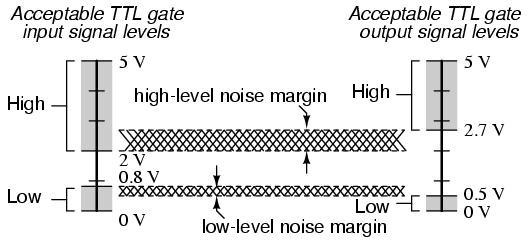
TTL gates operate on a nominal power supply voltage of 5 volts, +/- 0.25
volts. Ideally, a TTL "high" signal would be 5.00 volts exactly, and a TTL
"low" signal 0.00 volts exactly. However, real TTL gate circuits cannot
output such perfect voltage levels, and are designed to accept "high" and
"low" signals deviating substantially from these ideal values. "Acceptable"
input signal voltages range from 0 volts to 0.8 volts for a "low" logic
state, and 2 volts to 5 volts for a "high" logic state. "Acceptable" output
signal voltages (voltage levels guaranteed by the gate manufacturer over a
specified range of load conditions) range from 0 volts to 0.5 volts for a
"low" logic state, and 2.7 volts to 5 volts for a "high" logic state:

If a voltage signal ranging between 0.8 volts and 2 volts were to be sent
into the input of a TTL gate, there would be no certain response from the
gate. Such a signal would be considered uncertain, and no logic gate
manufacturer would guarantee how their gate circuit would interpret such a
signal.
As you can see, the tolerable ranges for output signal levels are
narrower than for input signal levels, to ensure that any TTL gate
outputting a digital signal into the input of another TTL gate will transmit
voltages acceptable to the receiving gate. The difference between the
tolerable output and input ranges is called the noise margin of the
gate. For TTL gates, the low-level noise margin is the difference between
0.8 volts and 0.5 volts (0.3 volts), while the high-level noise margin is
the difference between 2.7 volts and 2 volts (0.7 volts). Simply put, the
noise margin is the peak amount of spurious or "noise" voltage that may be
superimposed on a weak gate output voltage signal before the receiving gate
might interpret it wrongly:
CMOS gate circuits have input and output signal specifications that are
quite different from TTL. For a CMOS gate operating at a power supply
voltage of 5 volts, the acceptable input signal voltages range from 0 volts
to 1.5 volts for a "low" logic state, and 3.5 volts to 5 volts for a "high"
logic state. "Acceptable" output signal voltages (voltage levels guaranteed
by the gate manufacturer over a specified range of load conditions) range
from 0 volts to 0.05 volts for a "low" logic state, and 4.95 volts to 5
volts for a "high" logic state:
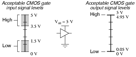
It should be obvious from these figures that CMOS gate circuits have far
greater noise margins than TTL: 1.45 volts for CMOS low-level and high-level
margins, versus a maximum of 0.7 volts for TTL. In other words, CMOS
circuits can tolerate over twice the amount of superimposed "noise" voltage
on their input lines before signal interpretation errors will result.
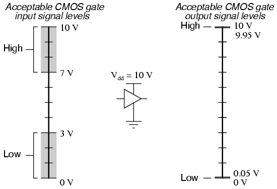
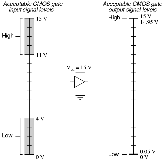
CMOS noise margins widen even further with higher operating voltages.
Unlike TTL, which is restricted to a power supply voltage of 5 volts, CMOS
may be powered by voltages as high as 15 volts (some CMOS circuits as high
as 18 volts). Shown here are the acceptable "high" and "low" states, for
both input and output, of CMOS integrated circuits operating at 10 volts and
15 volts, respectively:
The margins for acceptable "high" and "low" signals may be greater than
what is shown in the previous illustrations. What is shown represents
"worst-case" input signal performance, based on manufacturer's
specifications. In practice, it may be found that a gate circuit will
tolerate "high" signals of considerably less voltage and "low" signals of
considerably greater voltage than those specified here.
Conversely, the extremely small output margins shown -- guaranteeing
output states for "high" and "low" signals to within 0.05 volts of the power
supply "rails" -- are optimistic. Such "solid" output voltage levels will be
true only for conditions of minimum loading. If the gate is sourcing or
sinking substantial current to a load, the output voltage will not be able
to maintain these optimum levels, due to internal channel resistance of the
gate's final output MOSFETs.
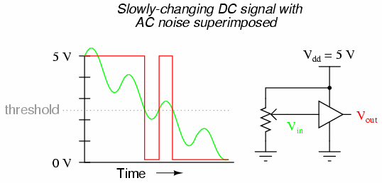
Within the "uncertain" range for any gate input, there will be some point
of demarcation dividing the gate's actual "low" input signal range from its
actual "high" input signal range. That is, somewhere between the lowest
"high" signal voltage level and the highest "low" signal voltage level
guaranteed by the gate manufacturer, there is a threshold voltage at which
the gate will actually switch its interpretation of a signal from
"low" or "high" or visa-versa. For most gate circuits, this unspecified
voltage is a single point:

In the presence of AC "noise" voltage superimposed on the DC input
signal, a single threshold point at which the gate alters its interpretation
of logic level will result in an erratic output:
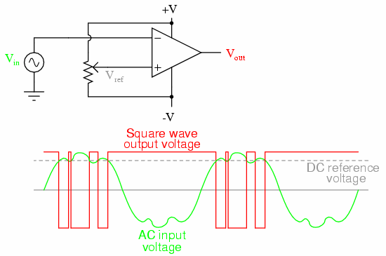
If this scenario looks familiar to you, it's because you remember a
similar problem with (analog) voltage comparator op-amp circuits. With a
single threshold point at which an input causes the output to switch between
"high" and "low" states, the presence of significant noise will cause
erratic changes in the output:
The solution to this problem is a bit of positive feedback
introduced into the amplifier circuit. With an op-amp, this is done by
connecting the output back around to the noninverting (+) input through a
resistor. In a gate circuit, this entails redesigning the internal gate
circuitry, establishing the feedback inside the gate package rather than
through external connections. A gate so designed is called a Schmitt
trigger. Schmitt triggers interpret varying input voltages according to
two threshold voltages: a positive-going threshold (VT+),
and a negative-going threshold (VT-):
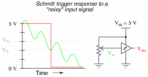
Schmitt trigger gates are distinguished in schematic diagrams by the
small "hysteresis" symbol drawn within them, reminiscent of the B-H curve
for a ferromagnetic material. Hysteresis engendered by positive feedback
within the gate circuitry adds an additional level of noise immunity to the
gate's performance. Schmitt trigger gates are frequently used in
applications where noise is expected on the input signal line(s), and/or
where an erratic output would be very detrimental to system performance.
The differing voltage level requirements of TTL and CMOS technology
present problems when the two types of gates are used in the same system.
Although operating CMOS gates on the same 5.00 volt power supply voltage
required by the TTL gates is no problem, TTL output voltage levels will not
be compatible with CMOS input voltage requirements.
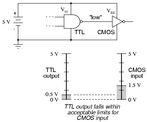
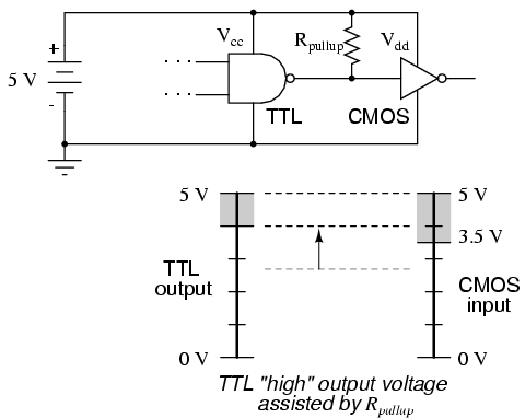
Take for instance a TTL NAND gate outputting a signal into the input of a
CMOS inverter gate. Both gates are powered by the same 5.00 volt supply (Vcc).
If the TTL gate outputs a "low" signal (guaranteed to be between 0 volts and
0.5 volts), it will be properly interpreted by the CMOS gate's input as a
"low" (expecting a voltage between 0 volts and 1.5 volts):
However, if the TTL gate outputs a "high" signal (guaranteed to be
between 5 volts and 2.7 volts), it might not be properly interpreted
by the CMOS gate's input as a "high" (expecting a voltage between 5 volts
and 3.5 volts):

Given this mismatch, it is entirely possible for the TTL gate to output a
valid "high" signal (valid, that is, according to the standards for TTL)
that lies within the "uncertain" range for the CMOS input, and may be
(falsely) interpreted as a "low" by the receiving gate. An easy "fix" for
this problem is to augment the TTL gate's "high" signal voltage level by
means of a pullup resistor:
Something more than this, though, is required to interface a TTL output
with a CMOS input, if the receiving CMOS gate is powered by a greater power
supply voltage:
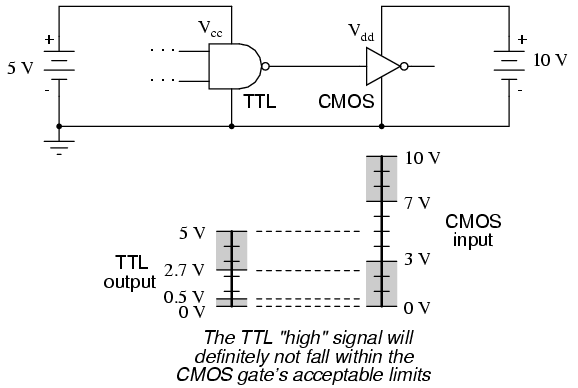
There will be no problem with the CMOS gate interpreting the TTL gate's
"low" output, of course, but a "high" signal from the TTL gate is another
matter entirely. The guaranteed output voltage range of 2.7 volts to 5 volts
from the TTL gate output is nowhere near the CMOS gate's acceptable range of
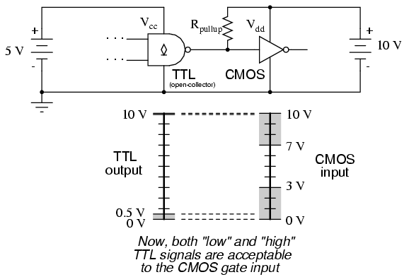
7 volts to 10 volts for a "high" signal. If we use an open-collector
TTL gate instead of a totem-pole output gate, though, a pullup resistor to
the 10 volt Vdd supply rail will raise the TTL gate's "high"
output voltage to the full power supply voltage supplying the CMOS gate.
Since an open-collector gate can only sink current, not source current, the
"high" state voltage level is entirely determined by the power supply to
which the pullup resistor is attached, thus neatly solving the mismatch
problem:
Due to the excellent output voltage characteristics of CMOS gates, there
is typically no problem connecting a CMOS output to a TTL input. The only
significant issue is the current loading presented by the TTL inputs, since
the CMOS output must sink current for each of the TTL inputs while in the
"low" state.
When the CMOS gate in question is powered by a voltage source in excess
of 5 volts (Vcc), though, a problem will result. The "high"
output state of the CMOS gate, being greater than 5 volts, will exceed the
TTL gate's acceptable input limits for a "high" signal. A solution to this
problem is to create an "open-collector" inverter circuit using a discrete
NPN transistor, and use it to interface the two gates together:
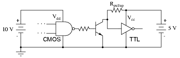
The "Rpullup" resistor is optional, since TTL inputs
automatically assume a "high" state when left floating, which is what will
happen when the CMOS gate output is "low" and the transistor cuts off. Of
course, one very important consequence of implementing this solution is the
logical inversion created by the transistor: when the CMOS gate outputs a
"low" signal, the TTL gate sees a "high" input; and when the CMOS gate
outputs a "high" signal, the transistor saturates and the TTL gate sees a
"low" input. So long as this inversion is accounted for in the logical
scheme of the system, all will be well. |
