While the binary numeration system is an interesting
mathematical abstraction, we haven't yet seen its practical application to
electronics. This chapter is devoted to just that: practically applying the
concept of binary bits to circuits. What makes binary numeration so
important to the application of digital electronics is the ease in which
bits may be represented in physical terms. Because a binary bit can only
have one of two different values, either 0 or 1, any physical medium capable
of switching between two saturated states may be used to represent a bit.
Consequently, any physical system capable of representing binary bits is
able to represent numerical quantities, and potentially has the ability to
manipulate those numbers. This is the basic concept underlying digital
computing.
Electronic circuits are physical systems that lend themselves well to the
representation of binary numbers. Transistors, when operated at their bias
limits, may be in one of two different states: either cutoff (no controlled
current) or saturation (maximum controlled current). If a transistor circuit
is designed to maximize the probability of falling into either one of these
states (and not operating in the linear, or active, mode), it can
serve as a physical representation of a binary bit. A voltage signal
measured at the output of such a circuit may also serve as a representation
of a single bit, a low voltage representing a binary "0" and a (relatively)
high voltage representing a binary "1." Note the following transistor
circuit:
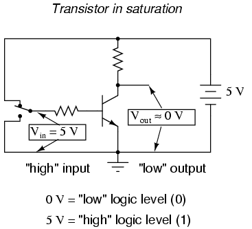 In this circuit, the transistor is in a state of saturation
by virtue of the applied input voltage (5 volts) through the two-position
switch. Because it's saturated, the transistor drops very little voltage
between collector and emitter, resulting in an output voltage of
(practically) 0 volts. If we were using this circuit to represent binary
bits, we would say that the input signal is a binary "1" and that the output
signal is a binary "0." Any voltage close to full supply voltage (measured
in reference to ground, of course) is considered a "1" and a lack of voltage
is considered a "0." Alternative terms for these voltage levels are high
(same as a binary "1") and low (same as a binary "0"). A general term
for the representation of a binary bit by a circuit voltage is logic
level.
Moving the switch to the other position, we apply a binary "0" to the
input and receive a binary "1" at the output:
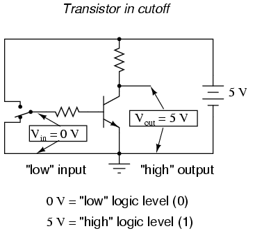 What we've created here with a single transistor is a
circuit generally known as a logic gate, or simply gate. A
gate is a special type of amplifier circuit designed to accept and generate
voltage signals corresponding to binary 1's and 0's. As such, gates are not
intended to be used for amplifying analog signals (voltage signals
between 0 and full voltage). Used together, multiple gates may be
applied to the task of binary number storage (memory circuits) or
manipulation (computing circuits), each gate's output representing one bit
of a multi-bit binary number. Just how this is done is a subject for a later
chapter. Right now it is important to focus on the operation of individual
gates.
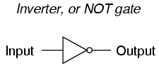
The gate shown here with the single transistor is known as an inverter,
or NOT gate, because it outputs the exact opposite digital signal as what is
input. For convenience, gate circuits are generally represented by their own
symbols rather than by their constituent transistors and resistors. The
following is the symbol for an inverter:
 An alternative symbol for an inverter is shown here:
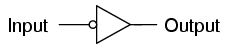 Notice the triangular shape of the gate symbol, much like
that of an operational amplifier. As was stated before, gate circuits
actually are amplifiers. The small circle, or "bubble" shown on either the
input or output terminal is standard for representing the inversion
function. As you might suspect, if we were to remove the bubble from the
gate symbol, leaving only a triangle, the resulting symbol would no longer
indicate inversion, but merely direct amplification. Such a symbol and such
a gate actually do exist, and it is called a buffer, the subject of
the next section.
Like an operational amplifier symbol, input and output connections are
shown as single wires, the implied reference point for each voltage signal
being "ground." In digital gate circuits, ground is almost always the
negative connection of a single voltage source (power supply). Dual, or
"split," power supplies are seldom used in gate circuitry. Because gate
circuits are amplifiers, they require a source of power to operate. Like
operational amplifiers, the power supply connections for digital gates are
often omitted from the symbol for simplicity's sake. If we were to show
all the necessary connections needed for operating this gate, the
schematic would look something like this:
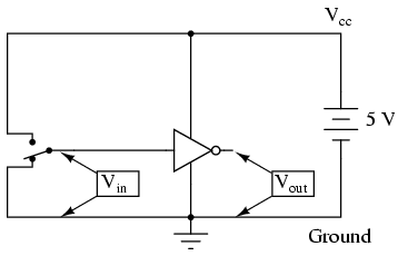 Power supply conductors are rarely shown in gate circuit
schematics, even if the power supply connections at each gate are.
Minimizing lines in our schematic, we get this:
 "Vcc" stands for the constant voltage supplied
to the collector of a bipolar junction transistor circuit, in reference to
ground. Those points in a gate circuit marked by the label "Vcc"
are all connected to the same point, and that point is the positive terminal
of a DC voltage source, usually 5 volts.
As we will see in other sections of this chapter, there are quite a few
different types of logic gates, most of which have multiple input terminals
for accepting more than one signal. The output of any gate is dependent on
the state of its input(s) and its logical function.
One common way to express the particular function of a gate circuit is
called a truth table. Truth tables show all combinations of input
conditions in terms of logic level states (either "high" or "low," "1" or
"0," for each input terminal of the gate), along with the corresponding
output logic level, either "high" or "low." For the inverter, or NOT,
circuit just illustrated, the truth table is very simple indeed:
 Truth tables for more complex gates are, of course, larger
than the one shown for the NOT gate. A gate's truth table must have as many
rows as there are possibilities for unique input combinations. For a
single-input gate like the NOT gate, there are only two possibilities, 0 and
1. For a two input gate, there are four possibilities (00, 01, 10,
and 11), and thus four rows to the corresponding truth table. For a
three-input gate, there are eight possibilities (000, 001, 010, 011,
100, 101, 110, and 111), and thus a truth table with eight rows are needed.
The mathematically inclined will realize that the number of truth table rows
needed for a gate is equal to 2 raised to the power of the number of input
terminals.
REVIEW: In digital circuits, binary bit values of 0 and 1 are represented by
voltage signals measured in reference to a common circuit point called
ground. An absence of voltage represents a binary "0" and the presence
of full DC supply voltage represents a binary "1." A logic gate, or simply gate, is a special form of
amplifier circuit designed to input and output logic level voltages
(voltages intended to represent binary bits). Gate circuits are most
commonly represented in a schematic by their own unique symbols rather
than by their constituent transistors and resistors. Just as with operational amplifiers, the power supply connections to
gates are often omitted in schematic diagrams for the sake of simplicity.
A truth table is a standard way of representing the
input/output relationships of a gate circuit, listing all the possible
input logic level combinations with their respective output logic levels.
|
