The single-transistor inverter circuit illustrated earlier
is actually too crude to be of practical use as a gate. Real inverter
circuits contain more than one transistor to maximize voltage gain (so as to
ensure that the final output transistor is either in full cutoff or full
saturation), and other components designed to reduce the chance of
accidental damage.
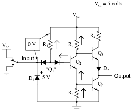
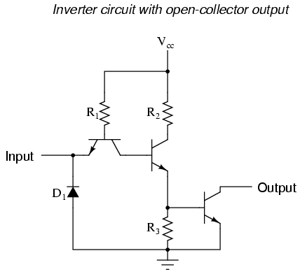
Shown here is a schematic diagram for a real inverter circuit, complete
with all necessary components for efficient and reliable operation:
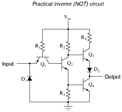 This circuit is composed exclusively of resistors and
bipolar transistors. Bear in mind that other circuit designs are capable of
performing the NOT gate function, including designs substituting
field-effect transistors for bipolar (discussed later in this chapter).
Let's analyze this circuit for the condition where the input is "high,"
or in a binary "1" state. We can simulate this by showing the input terminal
connected to Vcc through a switch:
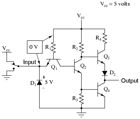 In this case, diode D1 will be reverse-biased,
and therefore not conduct any current. In fact, the only purpose for having
D1 in the circuit is to prevent transistor damage in the case of
a negative voltage being impressed on the input (a voltage that is
negative, rather than positive, with respect to ground). With no voltage
between the base and emitter of transistor Q1, we would expect no
current through it, either. However, as strange as it may seem, transistor Q1
is not being used as is customary for a transistor. In reality, Q1
is being used in this circuit as nothing more than a back-to-back pair of
diodes. The following schematic shows the real function of Q1:
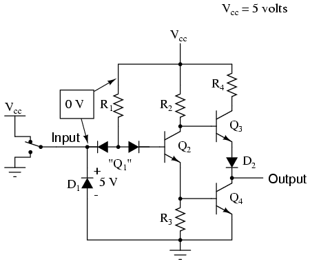 The purpose of these diodes is to "steer" current to or
away from the base of transistor Q2, depending on the logic level
of the input. Exactly how these two diodes are able to "steer" current isn't
exactly obvious at first inspection, so a short example may be necessary for
understanding. Suppose we had the following diode/resistor circuit,
representing the base-emitter junctions of transistors Q2 and Q4
as single diodes, stripping away all other portions of the circuit so that
we can concentrate on the current "steered" through the two back-to-back
diodes:
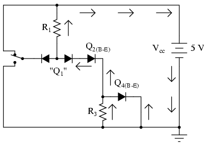
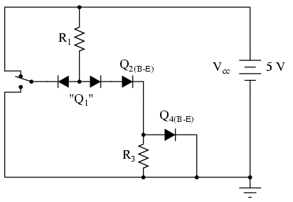 With the input switch in the "up" position (connected to Vcc),
it should be obvious that there will be no current through the left steering
diode of Q1, because there isn't any voltage in the
switch-diode-R1-switch loop to motivate electrons to flow.
However, there will be current through the right steering diode of Q1,
as well as through Q2's base-emitter diode junction and Q4's
base-emitter diode junction:
 This tells us that in the real gate circuit, transistors Q2
and Q4 will have base current, which will turn them on to conduct
collector current. The total voltage dropped between the base of Q1
(the node joining the two back-to-back steering diodes) and ground will be
about 2.1 volts, equal to the combined voltage drops of three PN junctions:
the right steering diode, Q2's base-emitter diode, and Q4's
base-emitter diode.
Now, let's move the input switch to the "down" position and see what
happens:
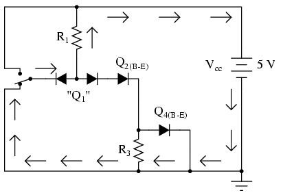 If we were to measure current in this circuit, we would
find that all of the current goes through the left steering diode of
Q1 and none of it through the right diode. Why is this? It
still appears as though there is a complete path for current through Q4's
diode, Q2's diode, the right diode of the pair, and R1,
so why will there be no current through that path?
Remember that PN junction diodes are very nonlinear devices: they do not
even begin to conduct current until the forward voltage applied across them
reaches a certain minimum quantity, approximately 0.7 volts for silicon and
0.3 volts for germanium. And then when they begin to conduct current, they
will not drop substantially more than 0.7 volts. When the switch in this
circuit is in the "down" position, the left diode of the steering diode pair
is fully conducting, and so it drops about 0.7 volts across it and no more.
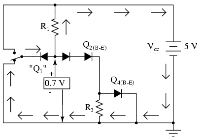 Recall that with the switch in the "up" position (transistors Q2
and Q4 conducting), there was about 2.1 volts dropped between
those same two points (Q1's base and ground), which also happens
to be the minimum voltage necessary to forward-bias three
series-connected silicon PN junctions into a state of conduction. The 0.7
volts provided by the left diode's forward voltage drop is simply
insufficient to allow any electron flow through the series string of the
right diode, Q2's diode, and the R3//Q4
diode parallel subcircuit, and so no electrons flow through that path. With
no current through the bases of either transistor Q2 or Q4,
neither one will be able to conduct collector current: transistors Q2
and Q4 will both be in a state of cutoff.
Consequently, this circuit configuration allows 100 percent switching of
Q2 base current (and therefore control over the rest of the gate
circuit, including voltage at the output) by diversion of current through
the left steering diode.
In the case of our example gate circuit, the input is held "high" by the
switch (connected to Vcc), making the left steering diode (zero
voltage dropped across it). However, the right steering diode is conducting
current through the base of Q2, through resistor R1:
 With base current provided, transistor Q2 will be turned "on."
More specifically, it will be saturated by virtue of the
more-than-adequate current allowed by R1 through the base. With Q2
saturated, resistor R3 will be dropping enough voltage to
forward-bias the base-emitter junction of transistor Q4, thus
saturating it as well:
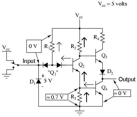 With Q4 saturated, the output terminal will be almost directly
shorted to ground, leaving the output terminal at a voltage (in reference to
ground) of almost 0 volts, or a binary "0" ("low") logic level. Due to the
presence of diode D2, there will not be enough voltage between
the base of Q3 and its emitter to turn it on, so it remains in
cutoff.
Let's see now what happens if we reverse the input's logic level to a
binary "0" by actuating the input switch:
 Now there will be current through the left steering diode of Q1
and no current through the right steering diode. This eliminates current
through the base of Q2, thus turning it off. With Q2
off, there is no longer a path for Q4 base current, so Q4
goes into cutoff as well. Q3, on the other hand, now has
sufficient voltage dropped between its base and ground to forward-bias its
base-emitter junction and saturate it, thus raising the output terminal
voltage to a "high" state. In actuality, the output voltage will be
somewhere around 4 volts depending on the degree of saturation and any load
current, but still high enough to be considered a "high" (1) logic level.
With this, our simulation of the inverter circuit is complete: a "1" in
gives a "0" out, and visa-versa.
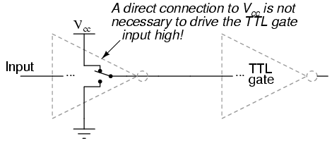
The astute observer will note that this inverter circuit's input will
assume a "high" state of left floating (not connected to either Vcc
or ground). With the input terminal left unconnected, there will be no
current through the left steering diode of Q1, leaving all of R1's
current to go through Q2's base, thus saturating Q2
and driving the circuit output to a "low" state:
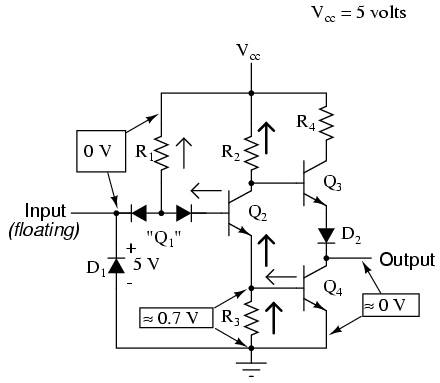 The tendency for such a circuit to assume a high input state if left
floating is one shared by all gate circuits based on this type of design,
known as Transistor-to-Transistor Logic, or TTL.
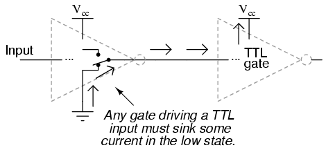
This characteristic may be taken advantage of in simplifying the design of a
gate's output circuitry, knowing that the outputs of gates typically
drive the inputs of other gates. If the input of a TTL gate circuit assumes
a high state when floating, then the output of any gate driving a TTL input
need only provide a path to ground for a low state and be floating for a
high state. This concept may require further elaboration for full
understanding, so I will explore it in detail here.
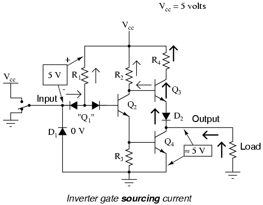
A gate circuit as we have just analyzed has the ability to handle output
current in two directions: in and out. Technically, this is known as
sourcing and sinking current, respectively. When the gate output
is high, there is continuity from the output terminal to Vcc
through the top output transistor (Q3), allowing electrons to
flow from ground, through a load, into the gate's output terminal, through
the emitter of Q3, and eventually up to the Vcc power
terminal (positive side of the DC power supply):
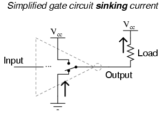
 To simplify this concept, we may show the output of a gate circuit as being
a double-throw switch, capable of connecting the output terminal either to Vcc
or ground, depending on its state. For a gate outputting a "high" logic
level, the combination of Q3 saturated and Q4 cutoff
is analogous to a double-throw switch in the "Vcc" position,
providing a path for current through a grounded load:
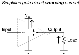 Please note that this two-position switch shown inside the gate symbol is
representative of transistors Q3 and Q4 alternately
connecting the output terminal to Vcc or ground, not of
the switch previously shown sending an input signal to the gate!
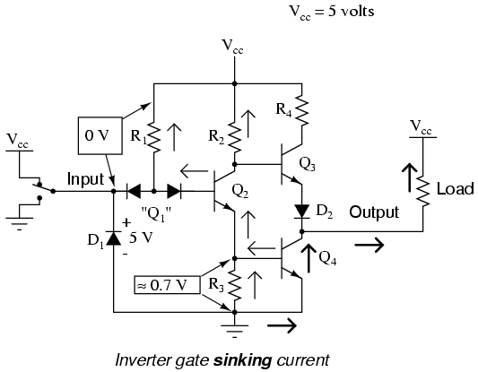
Conversely, when a gate circuit is outputting a "low" logic level to a
load, it is analogous to the double-throw switch being set in the "ground"
position. Current will then be going the other way if the load resistance
connects to Vcc: from ground, through the emitter of Q4,
out the output terminal, through the load resistance, and back to Vcc.
In this condition, the gate is said to be sinking current:
 The combination of Q3 and Q4 working as a "push-pull"
transistor pair (otherwise known as a totem pole output) has the
ability to either source current (draw in current to Vcc) or sink
current (output current from ground) to a load. However, a standard TTL gate
input never needs current to be sourced, only sunk. That is, since a
TTL gate input naturally assumes a high state if left floating, any gate
output driving a TTL input need only sink current to provide a "0" or "low"
input, and need not source current to provide a "1" or a "high" logic level
at the input of the receiving gate:
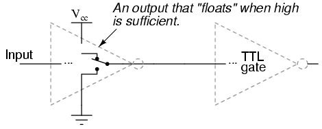
 This means we have the option of simplifying the output stage of a gate
circuit so as to eliminate Q3 altogether. The result is known as
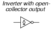
an open-collector output:
 To designate open-collector output circuitry within a standard gate symbol,
a special marker is used. Shown here is the symbol for an inverter gate with
open-collector output:
 Please keep in mind that the "high" default condition of a floating gate
input is only true for TTL circuitry, and not necessarily for other types,
especially for logic gates constructed of field-effect transistors.
REVIEW: An inverter, or NOT, gate is one that outputs the opposite state as
what is input. That is, a "low" input (0) gives a "high" output (1), and
visa-versa. Gate circuits constructed of resistors and bipolar transistors as
illustrated in this section are called TTL. TTL is an acronym
standing for Transistor-to-Transistor Logic. There are other design
methodologies used in gate circuits, some which use field-effect
transistors rather than bipolar transistors. A gate is said to be sourcing current when it provides a path
for current between the output terminal and the positive side of the DC
power supply (Vcc). In other words, it is connecting the output
terminal to the power source (+V). A gate is said to be sinking current when it provides a path
for current between the output terminal and ground. In other words, it is
grounding (sinking) the output terminal. Gate circuits with totem pole output stages are able to both
source and sink current. Gate circuits with open-collector
output stages are only able to sink current, and not source current.
Open-collector gates are practical when used to drive TTL gate inputs
because TTL inputs don't require current sourcing.
|
