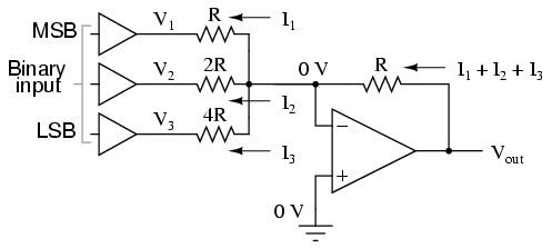
This DAC circuit, otherwise known as the
binary-weighted-input DAC, is a variation on the inverting summer op-amp
circuit. If you recall, the classic inverting summer circuit is an
operational amplifier using negative feedback for controlled gain, with
several voltage inputs and one voltage output. The output voltage is the
inverted (opposite polarity) sum of all input voltages:
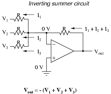
For a simple inverting summer circuit, all resistors must be of equal
value. If any of the input resistors were different, the input voltages
would have different degrees of effect on the output, and the output voltage
would not be a true sum. Let's consider, however, intentionally setting the
input resistors at different values. Suppose we were to set the input
resistor values at multiple powers of two: R, 2R, and 4R, instead of all the
same value R:
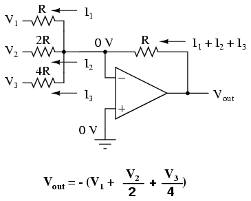
Starting from V1 and going through V3, this would
give each input voltage exactly half the effect on the output as the voltage
before it. In other words, input voltage V1 has a 1:1 effect on
the output voltage (gain of 1), while input voltage V2 has half
that much effect on the output (a gain of 1/2), and V3 half of
that (a gain of 1/4). These ratios are were not arbitrarily chosen: they are
the same ratios corresponding to place weights in the binary numeration
system. If we drive the inputs of this circuit with digital gates so that
each input is either 0 volts or full supply voltage, the output voltage will
be an analog representation of the binary value of these three bits.
If we chart the output voltages for all eight combinations of binary bits
(000 through 111) input to this circuit, we will get the following
progression of voltages:
Binary |
Output voltage |
000 |
0.00 V |
001 |
-1.25 V |
010 |
-2.50 V |
011 |
-3.75 V |
100 |
-5.00 V |
101 |
-6.25 V |
110 |
-7.50 V |
111 |
-8.75 V |
Note that with each step in the binary count sequence, there results a
1.25 volt change in the output. This circuit is very easy to simulate using
SPICE. In the following simulation, I set up the DAC circuit with a binary
input of 110 (note the first node numbers for resistors R1, R2,
and R3: a node number of "1" connects it to the positive side of
a 5 volt battery, and a node number of "0" connects it to ground). The
output voltage appears on node 6 in the simulation:
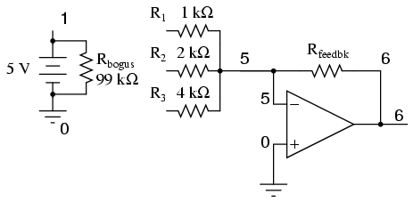
binary-weighted dac |
v1 1 0 dc 5 |
rbogus 1 0 99k |
r1 1 5 1k |
r2 1 5 2k |
r3 0 5 4k |
rfeedbk 5 6 1k |
e1 6 0 5 0 999k |
end |
node voltage node voltage node voltage |
(1) 5.0000 (5) 0.0000 (6) -7.5000 |
We can adjust resistors values in this circuit to obtain output voltages
directly corresponding to the binary input. For example, by making the
feedback resistor 800 Ω instead of 1 kΩ, the DAC will output -1 volt for the
binary input 001, -4 volts for the binary input 100, -7 volts for the binary
input 111, and so on.
(with feedback resistor set at 800 ohms)
|
Binary |
Output voltage |
|
000 |
0.00 V |
|
001 |
-1.00V |
|
010 |
-2.00 V |
|
011 |
-3.00 V |
|
100 |
-4.00 V |
|
101 |
-5.00 V |
|
110 |
-6.00 V |
|
111 |
-7.00 V |
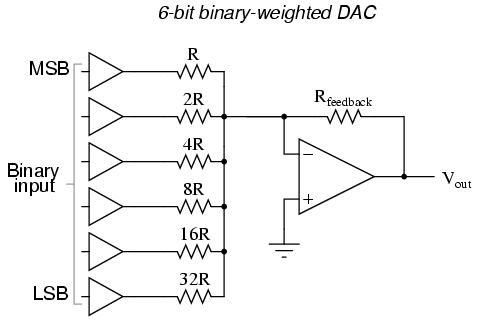
If we wish to expand the resolution of this DAC (add more bits to the
input), all we need to do is add more input resistors, holding to the same
power-of-two sequence of values:
It should be noted that all logic gates must output exactly the same
voltages when in the "high" state. If one gate is outputting +5.02 volts for
a "high" while another is outputting only +4.86 volts, the analog output of
the DAC will be adversely affected. Likewise, all "low" voltage levels
should be identical between gates, ideally 0.00 volts exactly. It is
recommended that CMOS output gates are used, and that input/feedback
resistor values are chosen so as to minimize the amount of current each gate
has to source or sink. |
