An alternative to the binary-weighted-input DAC
is the so-called R/2R DAC, which uses fewer unique resistor values. A
disadvantage of the former DAC design was its requirement of several
different precise input resistor values: one unique value per binary input
bit. Manufacture may be simplified if there are fewer different resistor
values to purchase, stock, and sort prior to assembly.
Of course, we could take our last DAC circuit and modify it to use a
single input resistance value, by connecting multiple resistors together in
series:
Unfortunately, this approach merely substitutes one type of complexity
for another: volume of components over diversity of component values. There
is, however, a more efficient design methodology.
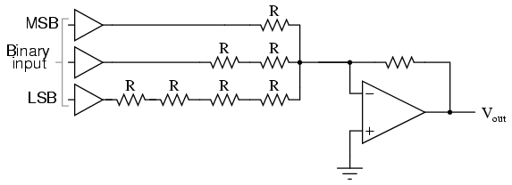
By constructing a different kind of resistor network on the input of our
summing circuit, we can achieve the same kind of binary weighting with only
two kinds of resistor values, and with only a modest increase in resistor
count. This "ladder" network looks like this:

Mathematically analyzing this ladder network is a bit more complex than
for the previous circuit, where each input resistor provided an
easily-calculated gain for that bit. For those who are interested in
pursuing the intricacies of this circuit further, you may opt to use
Thevenin's theorem for each binary input (remember to consider the effects
of the virtual ground), and/or use a simulation program like SPICE to
determine circuit response. Either way, you should obtain the following
table of figures:
|
Binary |
Output voltage |
|
000 |
0.00 V |
|
001 |
-1.25 V |
|
010 |
-2.50 V |
|
011 |
-3.75 V |
|
100 |
-5.00 V |
|
101 |
-6.25 V |
|
110 |
-7.50 V |
|
111 |
-8.75 V |
As was the case with the binary-weighted DAC design, we can modify the
value of the feedback resistor to obtain any "span" desired. For example, if
we're using +5 volts for a "high" voltage level and 0 volts for a "low"
voltage level, we can obtain an analog output directly corresponding to the
binary input (011 = -3 volts, 101 = -5 volts, 111 = -7 volts, etc.) by using
a feedback resistance with a value of 1.6R instead of 2R. |
